
Reverse Engineering using Pixel Images and Gerber files
 Using Pixel Images:
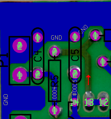
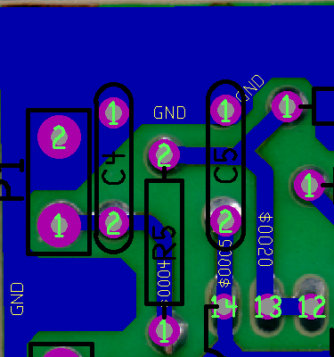
The power to have scanned images zoom and pan with the screen enables the user to "reverse engineer" a circuit board by simply scanning it, and then placing tracks and components on top of the scanned image. "Tracing" the original design in this manner is not only fast and efficient, but it leaves little chance for error. By comparing the image on the left with the image on the right it is easy to see how elementary of a process this is. The image on the left has had the track near the artificial red arrow deleted so that you are able to see the scanned "track" below it. Once the PCB reconstruction is complete, you can create a netlist and import it into a schematic file to start the process of rebuilding the schematic. As scanners have an inherent amount of inaccuracy in the optical axis, CIRCAD has an entire complement of pixel imaging functions that ensure you will have the ability to produce the most accurate source data from your scanned images. Expansion/contraction, and micro degree rotation functions ensure that an image is aligned accurate to within one thousandth of an inch. Controlling the color used to scan, as well as the utilization of high resolution images assists the user in achieving the ultimate image for reverse engineering of any given project. The process of scanning a green circuit board with only slightly darker green tracks yields an image with very little contrast. To correct for such problems, CIRCAD comes with powerful gamma control functions that can pull a usable image out of almost nothing. CIRCAD can also export your schematic drawings and circuit boards as graphics files at any zoom scale and any dpi, making documentation or web publishing your design a snap. |
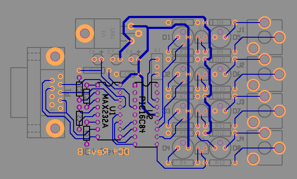
Multiple GERBER files can be read into a single on screen file. The process of tracing the design by placing tracks and components on top of the gerber files is very similar to the process for scanned images. Individual GERBER files may be released or have their display turned off to help eliminate confusion as the reverse engineering process takes place. In this example the source GERBER files have been read in to a blank PCB file. U1, U2, and capacitors C1 - C4 have been placed. Also, all of the bottom side tracks have been reconstructed. To finish the process you would simple place the remaining components and delete the GERBER files from the PCB. |