Building your own schematic components
Step 1:
Build the component outline with line segments, arcs, text labels, or what ever primitive elements that the component may need. These
must be placed on the Symbols layer. Place pads on the Master layer of type T0 = Schematic where the schematic
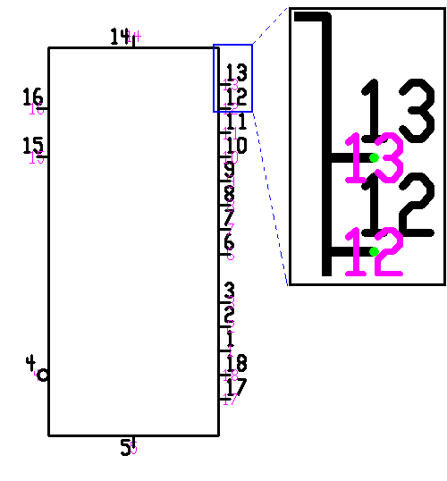
signal wires are to connect to the component. Be sure to place the pin numbers on the Pin Numbers layer. The numbers in
purple are the pin numbers displayed by the pad itself. They will not appear if the "Pin names/numbers" option is not selected in the
Setup Draw Modes.
Step 2:
Place 3 text strings that are literally &1, &2, and &3. These will be used to display data after the
component has been built. The &1 will be replaced by the reference identifier, the &2 will be replaced by the type/value, and the
&3 will be replaced by the type/value.

Step 3:
Place any additional documentation that may be desired. Be sure to place the pin names on the Pin Names layer. All other elements
should be place on the symbols layer.

Step 4: Block the entire component setting the reference point of the block as the place that the component is to be grabbed from.
The block can be as large as you desire as long as it contains all of the elements of the component and nothing else.

Step5:
Type <BB> or select Build Component from the Block menu. In the PCB pattern field enter the name of the PCB component that
is to be associated with this component.
